Q-Plus Labs

Sitemap | Contact Us 

Dimensional Measurement Blog

Q-PLUS Labs' Case Study: Extreme Components, LP's Surface Finish Analysis of DAT Mold Interlocks

Posted by Mike Knicker on Aug 12, 2016 12:47:02 PM

 banner_extreme-components.jpg

Extreme Components, LP is known for designing and creating cost-saving, effective alignment/positioning devices for the Injection Mold Industry that are durable, reliable, and high precision. Their molding alignment locks are manufactured using dynamic alignment technology or DAT, which is a revolutionary method for self-aligning locks that involves minimal friction and wear, even at high speeds. Using Q-PLUS Labs’ nano measurement expertise, Extreme Components, LP wanted to use the surface finish analysis results to find out precisely how well their DAT locks held up against the wear of daily use versus the traditional friction-fit locks.

Introduction

Extreme Components, LP's unique product was designed using DAT which consists of rollers constrained in a cage, and moving in a prescribed manner due to the kinematic relationship between the rollers. The tongue is moved relative to the housing without direct mechanical contact between the tongue and the housing. Because there is very minimal friction between parts, the process decreases the amount of wear that would normally be experienced using methods such as those used with traditional friction-fit locks.

Our Process

Color_Map.jpgTo analyze the exact amount of wear, Q-PLUS Labs performed a surface roughness analysis to confirm the wear on the unused surface of a traditional friction-fit lock versus the wear experienced by Extreme Components LP’s DAT locks after multiple uses. This was accomplished using white light profilometry from CyberTechnologies’ CT 300. The subsequent data from the unused surface of a friction-fit lock revealed an average roughness of 10.6 micro inches. There was major deviation from the level surface while the actual tongue contact surface was too rough to measure using conventional high precision instruments due to galling, or wear caused by adhesion between sliding surfaces, which could be observed from visual inspection.

Color_Map_EC.jpgIn comparison to the friction-fit lock, Extreme Components’ DAT lock that had been used by a multinational medical device manufacturer for 4 years of near continuous service, cycling every seven seconds with a 2,300 pound load yielding more than 10 million cycles, was measured to have a surface roughness of only 5.7 micro inches. The data of the surface map displays better uniformity than the friction-fit lock, and visual inspection shows the DAT lock’s mirror-like surface and no galling.

Usually, this measurement was done using far less accurate and time consuming means. However, with the rapid and accurate surface finish analysis data Q-PLUS Lab’s provided, Extreme Components was not only able to effectively compare their DAT locks to traditional friction-fit locks, but visually show customers the value of how their product holds up in real use scenarios.

 
New Call-to-action


Read More

Topics: manufacturing, 3D scanners, 3D Scanning, 3D scanning equipment, case studies, nano measurement,, CT300, nano

Nano measurements: Contact-based vs optical-based, which should you choose?

Posted by Mike Knicker on Jul 13, 2016 2:36:31 PM

Nano-measurements-Contact-based_vs_optical-based_which_should_you_choose.jpg

With advances in the manufacturing of smaller and smaller components, there is a need for measurements at that scale to ensure that best accuracy is maintained. If you require measurement at the nano scale, or one billionth of a meter, then choosing the right technology will be high on your priority list. You want to make the most informed decision when choosing the equipment for measurements that are this important.

In general, there are two different types of nano-measurement technology, contact-based and optical-based. Here is a bit about each type of nano-measurement technology to help you determine which measurement option is the best fit for your application:

How do contact-based nano-measurements work?

1_2D_Image2.jpg
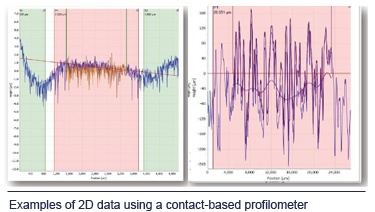
As the name suggests, this type of nano measurement solution will come in contact with the piece to be measured in order to determine its dimensions. The two main types of equipment capable of these measurements are stylus profilometers and the atomic force microscope. Both have been in use for some time and use extremely sensitive styluses to collect the measurement data required.

This type of nano-measurement is ideal if you need to measure a surface with a high aspect ratio since this can be a difficult to accomplish with optical-based solutions. These solutions have been around for a while so they are a tried and true way of measuring, and these methods are practically good at delivering 2-D data.

How do optical-based nano-measurements work?

1_3D_Image2.jpg
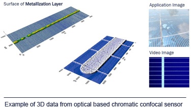
Optical-based nano-measurement technologies are quickly becoming the go-to devices for measurements at the nano level. Since these techniques do not touch the surface of the piece to be measured, there is no risk that small or delicate parts will be damaged or moved during measurement. As an added feature, optical measurements are also done more quickly than traditional contact-based measurements, and typically have an innate ability to obtain 3D measurements in addition to 2D data.

There are several methods used in optical-based nano-measurement; among them are triangulation, white light interferometry, confocal microscopes and chromatic confocal sensors. The commonality of these methods is the use of light that is emitted and then re-captured in a manner that will allow the equipment to make the extremely accurate measurements necessary to measure at the nano level.

Which type of nano-measurement is right for you?

Each of the methods listed above has benefits and drawbacks that you will need to weigh in your decision; and the decision greatly depends on what you will be measuring. As stated, contact-based measurements can make very high resolution measurements because they come in contact with the surface, but this also risks damage for delicate parts and can be much more expensive to operate.

By contrast, optical-based measurements do not risk damage to parts as only light comes in contact with the pieces, and are capable of measuring much more quickly that the contact-based methods. The drawback can be some difficulty with surfaces with high aspect ratios; such as surfaces with many features such as grooves, sharp edges, holes, steps, steep slopes or channels. So it is important to know what you will be measuring when you are choosing between the nano-measurement equipment available.

This is where the dedicated team at Q-PLUS Labs can help. Our experts have taken the time to know all the aspects of each piece of equipment best suited for each customer's application in order to recommend the best fit measurement equipment. Whether you need measurement services or help finding the right equipment for in-house measurements, our team can help. Contact us today to schedule a consultation.

New Call-to-action


Read More

Topics: dimensional measurement, 3D Scanning, nano measurement,, nanoscale,, dimensional measurement services, noncontact inspection, measurement equipment, nanometer

More than Meets the Eye: 3 Advancements in Nano Measurement that Improved the Quality of Manufacturing

Posted by Mike Knicker on Aug 26, 2015 2:21:44 PM

More than Meets the Eye: 3 Advancements in Nano Measurement that Improved the Quality of Manufacturing

Nanotechnology has matured from science fiction into a burgeoning industry and, now, to a well-accepted component of modern manufacturing. Many people don't realize just how much nanotechnology is involved, not just for high-tech electronics and aerospace, but also for everyday applications such as adhesives, printing, and automobiles. 

As measurement capabilities have expanded from the micro to the nano scale, there has been a corresponding improvement in the quality of manufacturing across many types of industries.

3 Advancements in Nano Measurement

With the ability to provide faster, accurate results necessary to monitor quality for products requiring micro manufacturing, developments in nano measurement technologies have introduced new possibilities for manufacturers. Some of the ways that nano measurement has improved the quality of manufacturing include:

  1. Electronics - Nano measurement is commonly used for applications such as checking the size, shape, and position of solder bumps on printed circuits and determining the thickness ratios of thin films on microelectromechanical systems (MEMS).

  2. Solar cells - Analysis and quality control of solar cell manufacturing have also been improved by developments in nano measurement. Nanocrystal solar cells have a very thin coating based on silicon or a similar substrate that has a uniform coating on the surface of the cell. This coating can only be analyzed using nano measurement to confirm uniform thickness.

  3. Medical diagnostics - Advances in nano measurement are helping researchers develop medical diagnostic tools that are more sensitive and produce consistently reliable results. There are several potential applications for nano measurement in the medical field, including targeted therapy of cardiac diseases, quantitative detection devices for early diagnosis of cancer, and the development of implantable devices for in vivo diagnoses.

Because the field of nano technology is developing at an exponential level, selecting the right nano measurement device (or combination of devices) for a particular surface profilometrydimensional inspection, or reverse engineering application requires careful consideration to ensure that you receive relevant results in the necessary time frame and within your budget. The experts at Q-PLUS Labs will work closely with you to determine the best solution for you application. Contact us today to schedule a consultation.

New Call-to-action


Read More

Topics: nano measurement,, nano scanning,, nanoscale,

What Types of Data Can Be Obtained from Nano Measurement?

Posted by Mike Knicker on Aug 11, 2015 2:01:00 PM

What Types of Data Can Be Obtained from Nano Measurement

Dimensional inspection is employed to measure a broad range of sample types in almost every industry imaginable. This same versatility is required at the nano scale, which is why ongoing effort is put into the development of new measurement technologies.

The combination of stylus profilometers, chromatic confocal technology, interferometry, and other types of sensors enables the collection of multiple types of data at the nano level. The ability to use various sensor types, sometimes even for the same sample, makes measuring objects with varying characteristics possible. For example, although using a stylus profilometer to measure an object with a soft surface may not be possible, an optical sensor can solve the problem.

Types of Nano Measurements

Some of the types of measurements that can be obtained at the nano scale include:

  • Form -  Micro gears and other small parts require precision shapes and contours. Complex 2D and 3D geometry can be captured at the nano scale with sensors that capture and process point cloud data.

  • Roughness - Surface roughness is one of the most common applications for nano measurement. In this case, the type of measurement technology used will depend on the height difference between the highest and lowest points on the surface, whether the material is hard or soft, and the type of results required for the application in 2D or 3D.

  • Flatness - The flatness of a pane of glass or man-made sapphire can be measured, regardless of the reflectivity of the surface. When chromatic confocal technology is employed, even the flatness of the opposite side of the glass can also be measured through the translucent material.

  • Coplanarity - For a Ball Grid Array (BGA), the top of each solder ball needs to be coplanar with all the others so the mating component seats properly and all connections are made. The geometry of these parts can be measured and verified at the nano scale.

  • Roundness - Micro gears and other small parts require precision shapes and contours. The geometry of these parts can be measured and verified at the nano scale.

  • Thickness - The thickness of wafers, plastic films, and epoxy films are examples of applications for which nano measurement is often employed. With a chromatic confocal sensor, the thickness of translucent objects, like the glass face of a smartphone, can be determined.

These are not the only types of measurements that can be obtained at the nano scale. The use of multiple types of sensors and the ongoing development of new nano measurement technology are continually expanding the possibilities for manufacturers and researchers.

If you require any of these types of nano measurements, or if you're not sure what approach is needed, the experts at Q-PLUS Labs are here to help. We'll work closely with you through every step of the process to ensure that you get the best results for your application. Contact us anytime if you have questions, or when you're ready to get started.

New Call-to-action

Read More

Topics: dimensional inspection, nano measurement,, nano scanning,, optical sensor, nanoscale,, surface finish analysis,

How Nano Measurement Can Benefit Surface Finish Analysis

Posted by Mike Knicker on Jun 16, 2015 2:09:16 PM

    How Nano Measurement Can Benefit Surface Finish Analysis

Surface finish analysis is one of the most common applications of nano measurement, primarily because this field requires a high level of precision. Specialized equipment is necessary because traditional dimensional inspection technology is not able to capture surface characteristics such as texture, sharpness, flatness, and wear at the nano level. In many applications, the surface conditions are not important, but in some cases they can affect functionality; therefore, meeting certain specifications is critical.

In the past, 2D surface finish profilometers were one of the only ways to collect data and deliver topographical information. Although this data is useful, it imposes limitations on manufacturers and engineers because they are not able to verify specifications for 3D surface finishes.

The availability of newer nano measurement technologies is changing the landscape of surface finish analysis, making it possible to achieve full 3D analysis.

Nano Measurement and Surface Finish Analysis

Some of the features that nano measurement equipment is able to capture include:

  • Profile roughness - The profile roughness gives you 2D information about the texture of a surface. The data is collected along a single line or extracted from an area data collection.

  • Surface roughness - In this case, the roughness is measured across the entire area of the surface. This obviously provides more information than profile roughness because the characteristics are not necessarily the same over the entire surface of the object.

  • Wear measurements - The data that is collected can be compared with an existing data set to determine the amount of surface wear that has occurred on a part. This is important for high-precision manufacturing and other applications in which surface features affect functionality.

  • Volume measurements - The volumes of peaks, holes, pits, and bumps can be determined at the nano level. Minute differences in surface topography can have a major impact in applications such as solder points on micro circuit boards or artificial hip implants.

  • Finding defects - Identifying surface defects such as blemishes, holes, or scratches is an important part of quality control. When these defects occur at the nano level, the impact in certain applications can be significant. New nano measurement technologies not only have made identifying these surface defects possible, but also allow it to be achieved quickly, which is important in a fast-paced manufacturing environment.

Using a combination of technologies, Q-PLUS Labs can deliver simple surface finish readings, full 3D analyses with visualizations, raw point cloud data, and even fully parametric 3D CAD models of very small and complex geometry at the nano level. If you are looking for a provider that offers a wide variety of high-precision nano measurement, contact us today to get started.

New Call-to-action


Read More

Topics: nano measurement,, nano scanning,, nanoscale,, surface finish analysis,

3 Nano Measurement Basics

Posted by Mike Knicker on Jun 3, 2015 11:51:00 AM

3 Nano Measurement Basics

As a manufacturing executive or quality control director, you don't always need to understand the rigorous details of every procedure that occurs during or after the production process. In fact, the necessary steps are sometimes so specialized that outsourcing them to a qualified provider makes more sense. Dimensional inspection is a good example of this because of the level of expertise and different types of equipment that are required.

Dimensional measurement at the nano scale is a constantly evolving field. Although you might not need to know the intricacies of the technology, it helps to understand the basics.

3 Nano Measurement Basics for Manufacturers

  1. Understanding the scale - A nanometer is one billionth of a meter. This is a simple definition but is difficult for many people to envision. If you change the scale to imagine Earth as one meter, a tennis ball would be the equivalent of a nanometer. You can also think of it in terms of the diameter of the head of a pin, which is typically about one millimeter, or one million nanometers.
    With dimensional inspection, the devices that are used to measure small objects, even those at the micro scale, are not capable of accurately measuring at the nano scale. For example, you might be able to get accurate information about the contours of a pin, but you can't necessarily use the same device to determine its surface roughness.

  1. Measuring with stylus profilometers - Contact-based measurement systems are used for a broad range of dimensional inspection applications, including some at the nano scale. High-precision contact measurement devices use a needle-shaped stylus that is dragged across the surface of the sample to gather point data, which can then be used to render a 2D cross-section or even a 3D surface with precision in the tens of nanometers. Contact styli rely on touch to gather data, which is not appropriate for all types of objects, especially those that are soft or could potentially be damaged during the measurement process.

  1. Measuring with light - Light-based measuring devices can be employed to overcome the limitations of stylus profilometers. These do not rely on a physical stylus, but rather use different types of light, lenses, and sensors to collect measurement information. In general, light-based measurement systems are faster and more accurate than contact-based alternatives. Some devices can also measure reflective or transparent surfaces to determine, flatness, roughness, and other characteristics.

Higher-level manufacturing professionals must understand the limitations of nano measurement and that new technologies are emerging to overcome those limits. As both the speed and accuracy of nano measurement improve over time, new doors are constantly opening for innovators.

Most managers and executives find it too overwhelming or simply don't have the time to maintain a deep level knowledge about emerging technologies in nano measurement. This is why you rely on experts who are dedicated to staying current in their fields. If you want to learn more about nano measurement and how it might be applied in your business, contact the professionals at Q-PLUS Labs today.


New Call-to-action

Read More

Topics: nano measurement,, nano scanning,, nanoscale,

4 Nano Measurement Factors to Consider Before Purchasing Services

Posted by Mike Knicker on May 12, 2015 11:33:00 AM

3 Challenges that Come with Nano Measurement

Manufacturers in all types of industries often outsource metrology services to a qualified provider, including for nano measurement. This practice is common because purchasing equipment is expensive, there are ongoing costs to maintain it, and you must have qualified staff with the time to operate it.

Outsourcing gives you the benefits of expert technicians, experience with a broad range of applications, and access to multiple technologies. Like any service provider in any other industry, not all metrology labs are created equal. Take the time to evaluate each provider's capabilities before purchasing services, especially if you need help in the specialized field of nano measurement.

4 Nano Measurement Questions to Ask Service Providers

As you evaluate potential providers, consider the following factors:

  1. Can you effectively measure at the nano level? Not all metrology equipment is capable of gathering data at the nano level. Most modern dimensional inspection labs do offer services at the micro level, but even though that equipment can handle very small measurements, it is not necessarily suitable for nano applications.

  2. Will your sample fit in the device? Many of the devices used for collecting nano data have relatively small measurement envelopes. This works fine for microelectronics and dental brackets, but not well for larger samples such as panels with solar thin films.

  3. Will your sample be destroyed by the measurement technique? If you have a larger sample and your provider doesn't have the device to accommodate it, your only option might be to cut a section of the sample to get the data you need. Similarly, if the metrology lab intends to use a contact-based measurement system and your sample is sensitive, it might get damaged during the data collection process.

  4. Will you achieve the accuracy you need? Nano measurement is still relatively new in the world of dimensional inspection, and developments are emerging all the time. This means that a metrology lab that uses older technology is not likely to have the most cutting-edge equipment available. If you need measurement with a great degree of accuracy, make sure you ask the provider about the best resolution it can offer. A resolution of 20 or 30 nanometers is common for many devices, but new technologies have been able to achieve higher resolution.

Q-PLUS Labs offers outsourced measurement services at the nano level. We use several types of technology to deliver the best possible results, including skidless contact stylus systems, laser, chromatic confocal scanning, and more. If you're interested in learning more about our nano measurement services, contact us today.

New Call-to-action

Read More

Topics: nano measurement,, surface finish analysis,

How Nano Measurement Can Be Used in Dimensional Analysis

Posted by Mike Knicker on Apr 28, 2015 2:20:00 PM

How Nano Measurement Can Be Used in Dimensional Analysis

Dimensional analysis involves the comparison of a manufactured part or component to the specifications defined by engineering drawings, digital files and 3D CAD models, or a master tool or part. Historically, the scale of measurement capability has ranged from very large (airplane wings and automobile contours) to the micro level (printed circuit boards and micro electronics). However, as technology has evolved to include the development of manufacturing at the nano scale, dimensional analysis has needed to maintain the same pace.

Manufacturers and researchers have long been able to design parts with features or surface characteristics that can be specified at the nano level, but until recently, the technology did not exist to measure and validate at the same scale. The development of new equipment that uses a combination of different types of advanced technology to achieve greater accuracy at the nano scale is opening new doors for manufacturers to create the innovative products that they previously could not verify.

Nano Measurement in Dimensional Analysis

Some of the applications in which nano measurement can be applied in dimensional analysis include:

  • Precision valves
  • Medical blades
  • Orthodontics
  • Artificial joints
  • Inkjet cartridges
  • Printing and paper manufacturing

These are just a few examples of the many industries and applications that regularly use nano measurement to verify specifications, perform quality control tests, and reverse engineer parts.

Like other types of dimensional inspection, nano measurement can be performed to collect a broad range of data, including:

  • Surface roughness
  • Form
  • Flatness
  • Roundness
  • Sharpness
  • Step height
  • Wear
  • Texture
  • Defects

Results can be delivered in two or three dimensions, including full CAD renderings. Both contact and non-contact methods can be used, so almost any type of object can be effectively measured, including reflective surfaces.

In order to stay on the cutting edge of dimensional inspection, Q-PLUS Labs has kept pace with new nano measurement technologies. This means that we use the most advanced equipment available to provide accurate results with the highest resolution. If you are looking for outsourced nano measurement services, Q-PLUS Labs is an industry leader with a wide array of instruments and skilled professionals with expertise across many fields. Contact us today to learn more about our services.

New Call-to-action

Read More

Topics: nano measurement,, nano scanning,, nanoscale,

Top 7 Applications that Benefit from Nano Measurement

Posted by Mike Knicker on Apr 14, 2015 12:45:00 PM

Top 7 Applications that Benefit from Nano Measurement

The development of new ways to measure objects and surfaces at the nano scale has allowed dimensional inspection providers to improve both accuracy and speed. It has also enabled the measurement of larger samples and objects with different surface types, as well as provide better 3D imaging capability.

Advances in nano measurement are interesting from a scientific perspective, but they also offer practical benefits in a number of different areas.

7 Applications that Benefit from Nano Measurement

Some of the applications that can benefit from better nano measurement include:

  1. Dental - Orthodontic brackets with very small features are difficult to accurately measure with contact probes and vision systems. The use of chromatic confocal technology enables better data collection because stylus size is not an issue, it measures in 3D without contacting the part, and the results are not impacted by reflectivity or translucence.
  2. Forensics - The ability to measure fibers and tool marks with greater accuracy gives forensics professionals better resources when processing evidence. Even specimens without parametric geometry (such as tissue samples) can be modeled in 3D.
  3. Microelectronics - Circuit boards at the micro and nano scale must be measured for quality control to ensure that the conducting path is consistent with specifications and that the wire bonds are correctly oriented. Because the samples are so sensitive, they must not be destroyed during the measurement process, which is why a non-contact system is the best solution.
  4. Medical - Artificial joints, implants, and other medical devices require highly accurate surface geometry to perform at their best. Measuring surface form and roughness at the nano scale ensures that the specifications are met. Nano measurement can also be used in the development and manufacturing of surgical instruments.
  5. Printing - Nano measurement is used to determine the surface roughness of different types of paper. It can also be employed to analyze printing results and detect errors.
  6. Tools and machining - Micro tools and components require a high level of accuracy to operate correctly. Nano measurement can be used for detecting tiny flaws in a micro gear, for measuring form, or for determining the amount of wear on a part.
  7. Material science - The ability to accurately measure a broad range of surface types at the nano scale, without risk of damaging the sample, is a valuable addition to the material science industry. Even materials with differing reflective properties can be measured with the same device.

The list of potential applications goes on and on. Automobiles, injection molding, and plastic films are just a few more examples of the types of industries, processes, and products that can benefit from new nano measurement technologies.

Q-PLUS can help you with your nano measurement needs. We regularly work with businesses in almost every type of industry, so no matter what your application is, we have the experience and expertise you need to get accurate results. Contact us today to schedule your free consultation.

New Call-to-action

Read More

Topics: dimensional measurement, dimensional inspection, nano measurement,, nano scanning,, nanoscale,, surface finish analysis,

4 Challenges 3D Scanning Solves in Today’s Medical/Manufacturing Industry

Posted by Mike Knicker on Mar 31, 2015 1:00:00 PM

4 Challenges 3D Scanning Solves in Today’s Medical/Manufacturing Industry

3D scanning has evolved over the years from a slow process with relatively low precision to much faster, highly accurate technologies. The result is the application of 3D scanning in multiple industries, including the manufacturing of medical devices, surgical instruments, and other equipment for the healthcare field.

The advent of light-based scanning systems made it possible to collect data about soft tissues without the risk of damaging them or affecting the accuracy of measurement results with a contact probe. This opened new doors in the medical world and helped solve many challenges.

4 Medical/Manufacturing Problems Solved by 3D Scanning

A few examples of the impact of 3D scanning on the medical industry include:

  1. Better-fitting prosthetic devices - The human body has few flat surfaces with regular angles. This means that the prosthetic devices traditionally designed for amputees were difficult to properly size, thus resulting in patient discomfort and limited functionality. The ability to create 3D models of the free-form shapes of the body enables manufacturers to create custom prosthetic devices that conform to each patient's body.
  2. Better-designed prosthetic devices - In addition to fitting well, many patients want a prosthetic device that looks like a natural body part. Before non-contact 3D scanning, physicians would make a cast of a body part and develop a CAD model that would be used to make a custom prosthesis. Non-contact 3D scanning has enabled much faster data collection and significantly improved accuracy.
  3. Reverse engineering device parts - As artificial joints and other medical devices age, the components sometimes must be repaired or replaced. If there is no existing CAD model to replicate it, 3D scanning can be employed to reverse engineer a new part that matches, or to detect wear.
  4. Inspection and validation of devices - High-precision manufacturing is critical for certain types of devices, often at a very small scale. For example, parts such as  micro-valves, stents, and venous filters must have no defects and conform to highly detailed engineering specifications. 3D scanning can be used in a manufacturing environment to provide quality control both in-line and in batch inspection applications. Because results can be produced relatively quickly, the technology is also well suited for process validation.

The potential applications for 3D scanning in the healthcare industry are limitless. If you work in the medical manufacturing industry and need an outsourced 3D scanning provider, get in touch with Q-PLUS Labs today. We are also an authorized reseller of multiple device types from many different manufacturers and can help you set up a new 3D scanning system in your own lab.


New Call-to-action

Read More

Topics: nano measurement,, nano scanning,, nanoscale,